Search...
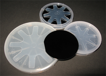

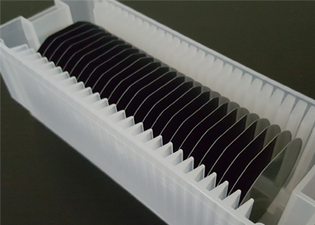

GaAs(Germanium Arsenide) Crystal and Substrates
Gallium Arsenide (GaAs) is a compound of the elements gallium and arsenic. It is a III-V direct bandgap semiconductor with a Zinc blende crystal structure.
Gallium Arsenide is used in the manufacture of devices such as microwave frequency integrated circuits, monolithic microwave integrated circuits, infrared light-emitting diodes, laser diodes, solar cells and optical windows. GaAs is often used as a substrate material for the epitaxial growth of other III-V semiconductors including indium gallium arsenide, aluminum gallium arsenide and others. And this kind of substrates has good performance under high frequency, high temperature and low temperature, low noise and high radiation tolerance.
 Video
Video


